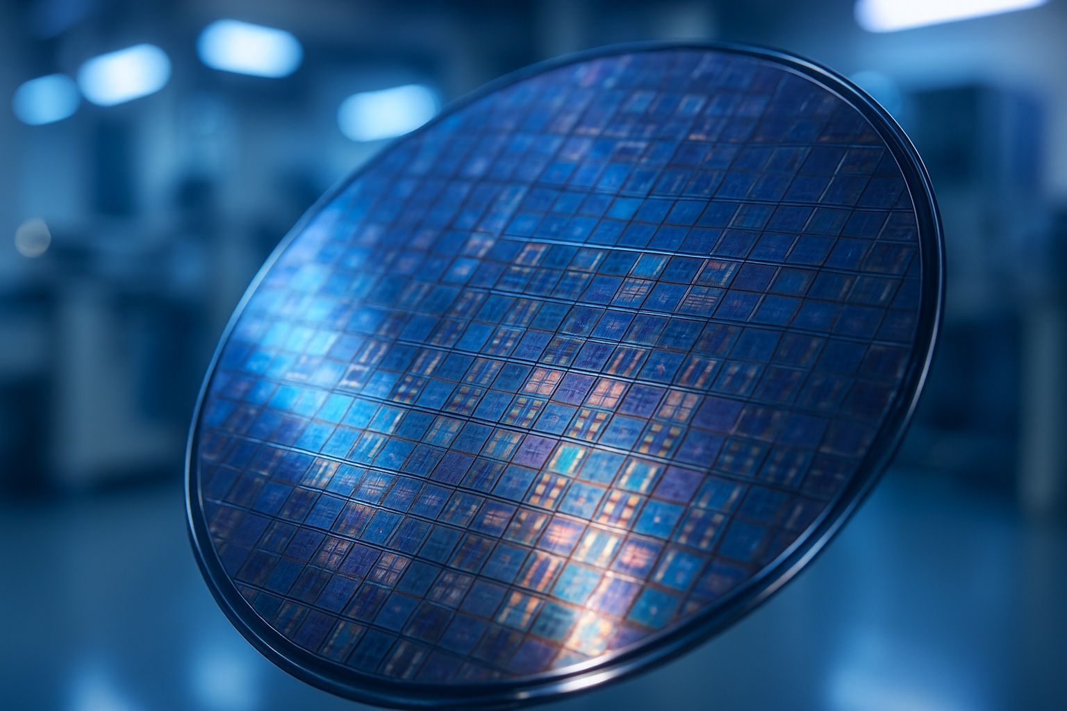
- In summer 2025, TSMC reported near 90% yield on its 3 nm process, versus Samsung’s roughly 50% yield.
- Samsung, which pioneered 3 nm gate-all-around transistors in 2022, continues to struggle with yields but has won Google’s Tensor G5 on 3 nm and other new clients for older nodes.
- TSMC and Samsung are racing toward 2 nm (N2-class) technology, with TSMC’s 2 nm on track for risk production and high-volume manufacturing in late 2025 or early 2026.
- Intel detailed an 18A process (approximately 1.8 nm class) at the mid-June VLSI Symposium, promising >30% logic density scaling and up to ~20% higher performance (or 36% power reduction) versus Intel’s 2023 Intel 3 node.
- Intel also revealed an SRAM cell size of 0.021 µm² on 18A, larger than TSMC’s planned 0.0175 µm² bitcell on N2.
- The first 18A product, a Panther Lake laptop CPU, is expected by late 2025 with volume ramp in 2026, around the same time AMD plans to launch chips on TSMC’s 2 nm in 2026.
- On June 12, TSMC and the University of Tokyo opened the TSMC-UTokyo Lab, TSMC’s first joint R&D lab with a university outside Taiwan.
- By mid-2025 ASML shipped five High-NA EXE:5000 EUV tools to Intel, TSMC, and Samsung for R&D, and Samsung installed its first High-NA unit at Hwaseong in March.
- TSMC said there is no compelling reason yet to deploy High-NA for its upcoming nodes and cites a price of about €350–€400 million per tool, delaying mass deployment.
- Micron announced a $200 billion US memory investment plan to build a second Boise mega-fab, expand Manassas, and possibly add two more fabs, supported by $275 million in CHIPS Act grants and expected to create up to 90,000 jobs.
Advanced Node Progress and Breakthroughs
The summer of 2025 saw significant strides in cutting-edge semiconductor process nodes. Taiwan Semiconductor Manufacturing Co. (TSMC) continued to lead in 3 nm production, reportedly achieving near 90% yield on its 3 nm process – far ahead of rival Samsung Foundry’s roughly 50% yield design-reuse.com. These yield discrepancies have driven more high-profile customers (like smartphone and GPU designers) toward TSMC, allowing it to command premium pricing design-reuse.com design-reuse.com. Samsung, which pioneered 3 nm gate-all-around (GAA) technology in 2022, still struggles to reach competitive yields and has even lost some mobile chip orders to TSMC, though it secured Google’s Tensor G5 on 3 nm and other new clients for older nodes design-reuse.com design-reuse.com.
Both TSMC and Samsung are now racing toward 2 nm (N2-class) technology. TSMC’s 2 nm is on track for risk production and aims for high-volume manufacturing (HVM) in late 2025 or early 2026 reuters.com reuters.com. Industry reports in June detailed a “fierce race” between TSMC and Samsung to debut 2 nm chips, with TSMC widely seen as ahead in yield and timing design-reuse.com. Samsung is prioritizing improvements to its 2 nm and 4 nm nodes and has reportedly postponed any 1.4 nm “trial line” investments, indicating its 1.4 nm node is unlikely to arrive before 2028–2029 design-reuse.com.
Meanwhile, Intel is executing on its aggressive roadmap. At the mid-June VLSI Symposium, Intel detailed performance gains for its upcoming 18A process (~1.8 nm class). According to a paper Intel presented, the 18A node offers >30% logic density scaling and up to ~20% higher performance (or 36% power reduction) compared to Intel’s 2023 “Intel 3” node bits-chips.com. This is achieved through a combination of gate-all-around (GAA) transistors, backside power delivery, advanced interconnects, and design co-optimization bits-chips.com. Intel also revealed an SRAM cell size of 0.021 µm² on 18A – comparable, though slightly larger, than TSMC’s planned 0.0175 µm² bitcell on N2 bits-chips.com. The first 18A product, a “Panther Lake” laptop CPU, is expected by late 2025 (with volume ramp in 2026), around the same time foundry clients like AMD plan to launch chips on TSMC’s 2 nm in 2026 bits-chips.com. These timelines underscore that the sub-2nm era is imminent, with multiple companies preparing to launch chips built on angstrom-class technologies in 2025–2026.
In research news, industry-academia collaborations and novel technologies also made headlines. In Japan, TSMC and the University of Tokyo formally opened the “TSMC-UTokyo Lab” on June 12 to advance semiconductor research and talent development design-reuse.com design-reuse.com. This is TSMC’s first joint R&D lab with a university outside Taiwan, aiming to leverage UTokyo’s expertise in materials, devices, and processes to drive innovations in areas like new transistor structures, metrology and packaging design-reuse.com design-reuse.com. On the academic front, European researchers debuted the world’s first 2D-material CMOS computer in mid-June – a laboratory demonstration highlighting potential future transistor materials beyond silicon (though such breakthroughs remain far from commercial deployment) bits-chips.com.
EUV Lithography: High-NA Era Begins
The transition to next-generation lithography took a step forward in this period with ASML’s High-NA EUV systems making their way into chipmakers’ fabs. ASML, the Dutch equipment maker and sole supplier of EUV scanners, has built a limited number of “EXE:5000” High-NA EUV machines (the first iteration of ~0.55 NA optics). By mid-2025, ASML had shipped five High-NA tools to three leading customers – Intel, TSMC, and Samsung – for R&D use reuters.com reuters.com. In fact, Samsung took delivery of its first high-NA EUV unit at Hwaseong in March, becoming the third chipmaker (after Intel and TSMC) with such a tool installed on-site bits-chips.com. All three companies (and others) also have access to a shared High-NA pilot tool at the ASML-IMEC lab in Veldhoven, which opened in late 2024 to accelerate process development on early High-NA hardware bits-chips.com bits-chips.com.
Despite this progress, chipmakers are approaching High-NA EUV cautiously. TSMC stated it has not yet found a “compelling reason” to use High-NA for its upcoming nodes and can extend immersion (0.33 NA) EUV a bit further reuters.com reuters.com. TSMC’s technology chief Kevin Zhang noted that the ~€350–400 million price of each High-NA tool (almost double a current EUV scanner) is hard to justify unless the benefit is clear reuters.com reuters.com. TSMC confirmed it will not deploy High-NA on its 2 nm generation (N2, also called “A16”), and possibly not even on the first enhancement of that node reuters.com reuters.com. Intel, by contrast, has publicly embraced High-NA: it plans to use an ASML High-NA machine for its Intel 14A process as early as 2026-27, in hopes of regaining process leadership reuters.com. Intel received its first High-NA tool and began initial assembly/tests this year, preparing for a 2026 pilot run reuters.com. Even so, Intel acknowledges customers may opt out if the tech is not mature, and ASML’s own guidance is that 2026–2027 will be spent proving High-NA in high-volume manufacturing, with wider adoption only in later advanced nodes reuters.com reuters.com.
ASML’s roadmap for EUV remains on track. The company is readying the second-gen High-NA tool (EXE:5200) for shipment “soon” – these production-grade machines will be needed for true volume fab insertion bits-chips.com. Industry watchers expect Intel to receive the first EXE:5200 units, as it targets late 2026/early 2027 for initial High-NA production use bits-chips.com. TSMC and Samsung have not announced mass-production timelines for High-NA, likely waiting for the EXE:5200 and a clearer cost/benefit picture. In the meantime, engineers are squeezing more from existing EUV: TSMC claims its baseline 0.33 NA EUV tools can support several more shrink iterations with tricks like multiple patterning and improved resists, delaying the urgent need for High-NA reuters.com reuters.com.
Other lithography and patterning innovations are also underway. Lam Research, a major etch equipment firm, is developing a dry resist technology for EUV lithography that could improve pattern resolution and simplify process steps by using novel deposition-etch techniques tradingview.com. And ASML hinted that even more radical solutions loom on the horizon – the company has been researching a “maskless” lithography scanner (potentially leveraging multi-beam or computational methods) as a future complement or successor to EUV bits-chips.com. While EUV will remain the workhorse for sub-5nm nodes, these advances in resist, etch, and even post-EUV patterning demonstrate the ecosystem’s push to keep Moore’s Law alive through the late 2020s.
Semiconductor Equipment Makers: Updates and Alliances
The world’s leading chip fabrication equipment suppliers – ASML, Applied Materials, Tokyo Electron, and Lam Research – navigated a complex landscape of booming technological demand and geopolitical headwinds during June–July 2025. ASML’s situation remains unique as its EUV tools are indispensable for the most advanced chips, but also subject to export controls (more on that in the policy section). Despite some cyclical softness in 2024, analysts expect ASML to rebound strongly in 2025 with ~20% revenue growth as orders for advanced lithography pick up seekingalpha.com. Indeed, ASML’s CEO said the company is on track for “huge growth” in 2025, driven by the ramp of 3nm/2nm fabs and early High-NA tool sales seekingalpha.com.
Other equipment firms are positioning around emerging trends. Applied Materials, the largest maker of deposition and etch tools, expanded a research partnership with CEA-Leti (France’s microelectronics research institute) on June 16. The joint lab will focus on materials engineering for specialty semiconductors – particularly aiming to develop more energy-efficient chips for AI and data centers ir.appliedmaterials.com. Applied is also investing in next-gen chip packaging: in early July, it announced a strategic stake in BE Semiconductor Industries (Besi), a Dutch advanced packaging equipment firm, acquiring ~9% of Besi’s shares globenewswire.com. This investment underscores how critical heterogeneous integration (chiplet and 3D packaging) has become, blurring the line between front-end fab and back-end assembly technologies.
Tokyo Electron (TEL), Japan’s top equipment supplier, struck an optimistic tone amid rising Chinese competition. TEL’s CEO publicly stated that the company is on course to widen its lead over Chinese chip tool makers despite billions in Chinese investment x.com. In late June, TEL noted that U.S. export restrictions are curbing its sales to China (forecasting its China revenue share to drop to ~30% this year) trendforce.com, but demand from elsewhere – particularly for tools enabling sub-2nm process development – remains robust. In one collaboration, TEL and Europe’s imec have extended their partnership to accelerate “beyond-2nm” node research, yielding breakthroughs in High-NA EUV patterning, etching, and deposition techniques for future transistors bisinfotech.com.
Likewise, Lam Research is innovating around EUV and memory scaling. The company’s new dry photoresist technology (introduced at SEMICON West 2025) is said to improve EUV resolution and reduce waste, combining plasma deposition and etch in one system tradingview.com. Lam is also reportedly working on next-gen etch solutions for 3D NAND, where layer counts now exceed 300+; rival TEL recently unveiled a potent new NAND etch tool as well tel.com. These advancements by equipment makers are crucial enablers for chipmakers’ roadmaps in logic and memory – from patterning those angstrom-scale transistors to drilling through skyscraper-like NAND stacks.
Advanced Packaging and Chiplet Innovations
With scaling becoming ever more challenging, the industry in mid-2025 placed increased emphasis on advanced packaging to keep performance growing. Both established companies and new entrants unveiled packaging-driven approaches to boost computing power:
- Huawei grabbed headlines in June with an ambitious chiplet-based AI processor design. The Chinese tech giant filed patents for a quad-chiplet “Ascend 910D” AI chip, aiming to rival Nvidia’s top GPUs via packaging prowess rather than cutting-edge lithography trendforce.com. The 910D would combine four identical chiplets in one package – a concept echoing Nvidia’s own multi-die “Rubin” GPU architecture trendforce.com. Huawei’s design uses bridge-style interconnects (similar to TSMC’s CoWoS-L or Intel’s EMIB/Foveros) instead of a large silicon interposer trendforce.com. If successful, this approach could allow Huawei to circumvent some U.S. sanctions by linking several less-advanced chips into a single powerful module trendforce.com. Analysts noted the chip could be enormous – potentially over 4,000 mm² of silicon in total when factoring in four compute dies plus 16 stacks of high-bandwidth memory (HBM) trendforce.com. While such a monster package would test the limits of current packaging tech (nearly five times the area of a single EUV reticle), it demonstrates how China’s players are leveraging advanced packaging to stay in the race trendforce.com trendforce.com.
- Industry-wide, chiplets and 2.5D/3D packaging are reshaping product roadmaps. BE Semiconductor (Besi), a key provider of die-bonding equipment, reported that an “accelerated adoption of 2.5D and 3D chiplet-based wafer-level structures” is underway as data-centric applications grow and traditional Moore’s Law slows bits-chips.com. Besi’s CEO highlighted that both logic and memory customers are turning to chiplet architectures, driving demand for advanced packaging solutions (such as high-density bumping, hybrid bonding, and wafer stacking) bits-chips.com. This trend prompted Besi to raise its long-term sales forecast substantially, reflecting optimism about the packaging market bits-chips.com. Indeed, major chipmakers like AMD and Intel are already delivering products with multiple dies in one package (for example, high-end PC CPUs with compute and I/O chiplets), and TSMC and Samsung now offer sophisticated foundry packaging services (CoWoS, InFO, X-Cube, I-Cube, etc.) to integrate HBM memory and chiplets for AI accelerators.
- Advanced packaging partnerships also emerged. In addition to the aforementioned Applied Materials-Besi tie-up, June saw reports that UMC (a Taiwanese foundry) is expanding advanced packaging capacity in cooperation with external partners trendforce.com. And in Europe, research consortiums under programs like EU Chip Acts are funding pilot lines for heterogeneous integration, recognizing packaging as a strategic capability. Even governments are getting involved: the U.S. CHIPS Act R&D arm is investing in packaging prototyping hubs, and Japan’s METI launched projects to advance chiplet standardization. All these efforts underscore a key point: packaging is the new battleground for performance. As one industry observer quipped, “advanced chip packaging now does more than protect—it boosts performance and efficiency,” becoming essential to next-gen CPUs, GPUs, and AI chips.
Market Outlook and Executive Commentary
Industry executives and analysts during this period offered generally upbeat – if cautious – forecasts for the semiconductor sector, especially for advanced technology nodes and AI-related demand:
- TSMC’s leadership expects strong growth returning in 2025 thanks to cutting-edge nodes. In an earnings call and subsequent statements, TSMC projected that “advanced technologies” (defined as 7 nm and below) will account for around 80% of its 2025 wafer revenue asiaconnectmagazine.com. The foundry noted booming interest in 3nm-class production for new smartphone SoCs and cloud AI accelerators, and it remained on schedule for 2 nm risk production. TSMC’s CEO C.C. Wei also highlighted that AI chips (for data centers) have become a key growth driver, creating entire new markets for its most advanced processes design-reuse.com. Supporting that, a mid-June analysis dubbed TSMC the “King of Data Center AI”, as the vast majority of cutting-edge AI chips (from companies like NVIDIA, Apple, and Amazon) are being manufactured on TSMC’s 5 nm and 4 nm lines, with 3 nm and 2 nm orders in the pipeline design-reuse.com.
- Samsung Electronics management, while lagging in foundry, pointed to bright spots in memory and packaging. Samsung’s memory division started sampling next-generation DDR5 and HBM4 memory, and is collaborating with partners on chiplet-friendly interfaces. Company officials believe their early adoption of GAA transistors at 3 nm will pay off at 2 nm. However, Samsung’s leadership privately acknowledged the need to improve yield and lure back foundry clients; the company initiated a talent shake-up by hiring a former TSMC executive to bolster its process engineering team in Texas dr-ipms.com. Samsung’s public statements affirmed a commitment to get 2 nm on line by 2025 and invest in 1.4 nm R&D, albeit on a longer timeline design-reuse.com.
- Intel’s CEO Pat Gelsinger and technology chief Ann Kelleher struck a confident tone about Intel’s path to regain process parity. They cited the on-time delivery of Intel 4 (7 nm) chips and the ahead-of-schedule progress on 20A and 18A nodes as evidence that Intel’s “five nodes in four years” plan is working. Intel is courting major fabless customers to its Intel Foundry Services (IFS) business, leveraging its upcoming 18A process (with High-NA EUV capability) as a selling point reuters.com. However, industry analysts caution that Intel’s success also hinges on software and packaging – hence Intel’s heavy investment in advanced packaging (e.g. its “EMIB” and “Foveros” technologies, which will also be offered to foundry clients).
- In Europe, a notable industry call to action came in May and echoed through early summer: SEMI’s European president urged the EU to quadruple its semiconductor funding commitment in the next budget cycle reuters.com reuters.com. The current €43 billion European Chips Act, largely backed by member states, is deemed insufficient to reach Europe’s goal of 20% global chip market share by 2030 reuters.com reuters.com. At the current pace, Europe might only reach ~11% share by 2030 reuters.com reuters.com. Executives from European firms like ASML and Infineon have similarly lobbied for “Chips Act 2.0” – a larger, pan-European fund to attract more fab projects. The summer saw incremental progress: EU authorities approved state aid for new semiconductor plants (including an Infineon-led power semiconductor fab in Dresden), and construction moved forward on Intel’s Magdeburg fab and TSMC’s joint venture fab in Germany, all aided by government incentives.
- Industry analysts remained bullish on segments like automotive and AI chips. Market researchers noted an upsurge in semiconductor capital spending; notably, China was expected to lead chipmaking equipment investment in 2025 with ~$38 billion (despite export controls), reflecting the construction of new memory fabs and mature-node foundries taipeitimes.com. At the same time, U.S. analysts predicted that AI-centric chips (GPUs, TPUs, accelerators) would be the fastest-growing chip segment through 2025, potentially offsetting weakness in smartphones and PCs. This optimism is tempered by supply chain considerations – e.g., NVIDIA’s CEO warned of potential supply constraints for AI GPUs if fab expansion or export policies don’t keep up with demand. Overall, the consensus by end of July was that the semiconductor downturn of 2023 had bottomed out, with recovery in 2024 and strong growth in 2025 led by bleeding-edge technologies and government-backed expansion.
Geopolitics and Policy: CHIPS Act, Export Curbs, and China’s Response
Government policy and geopolitical maneuvering had a profound impact on the semiconductor landscape in June–July 2025. In the United States, the new administration adjusted course on chip incentives and export controls:
- The CHIPS and Science Act – the $52.7 billion program to boost US chip manufacturing – underwent renegotiation of its grants. Commerce Secretary Howard Lutnick told Congress on June 4 that many Biden-era CHIP grant awards were “overly generous,” and the Trump administration is renegotiating them for better terms reuters.com reuters.com. Some deals might be canceled outright if deemed unnecessary. As an example, Lutnick cited TSMC’s Arizona project: originally promised $6 billion in federal grants, TSMC agreed to boost its US investment by $100 billion (from $65B to $165B) in exchange for keeping the same $6B incentive reuters.com reuters.com. This suggests TSMC will massively expand its Arizona fab cluster beyond the two fabs initially planned – a win that Lutnick framed as “more bang for the buck” for US taxpayers reuters.com reuters.com. (TSMC declined to comment on specifics.) Other recipients like Samsung, Intel, Micron, and SK Hynix are also under review, and the Commerce Dept. hinted that some awards may be reduced or delayed reuters.com reuters.com. The goal, per officials, is to ensure companies deliver greater domestic investment and capacity in return for subsidies.
- In parallel, major new domestic investments were announced. On June 12, the White House revealed a historic $200 billion investment plan by Micron Technology to expand memory chip manufacturing in the US nist.gov nist.gov. Micron, America’s only leading DRAM maker, will use this capital (spread over a decade or more) to build a second mega-fab in Boise, Idaho, expand its Manassas, Virginia fab (relocating some legacy DRAM tech from Taiwan to Virginia), and potentially add two additional fabs in upstate New York nist.gov nist.gov. The $200B commitment – one of the largest ever in chips – is supported by an incremental $275 million in CHIPS Act grants (on top of $6.1B Micron was awarded in late 2024 for earlier plans) nist.gov. Officials touted that these projects will create up to 90,000 jobs across states and “restore American chipmaking leadership,” especially in memory and advanced packaging (Micron will also build high-bandwidth memory packaging facilities) nist.gov nist.gov. This announcement was portrayed as a major victory for the Trump Administration’s “America First” agenda in tech nist.gov nist.gov.
- The U.S. also tightened export controls further, aiming to choke off China’s access to critical chipmaking inputs. In late May, the Commerce Department’s Bureau of Industry and Security quietly instructed companies that a broad range of tech will now require export licenses to ship to China reuters.com reuters.com. The new restrictions cover semiconductor design software (EDA tools), certain specialty chemicals used in chip fabrication, as well as other non-chip items like industrial machine tools and even some aviation parts reuters.com. Letters went out to EDA giants Cadence, Synopsys, and Siemens EDA informing them that any software exports to China will be subject to case-by-case licensing reuters.com reuters.com. This effectively puts China’s chip design houses on notice, as over 70% of EDA market share in China comes from those U.S. vendors reuters.com. Likewise, suppliers of high-end photoresists and materials received letters halting existing licenses. The U.S. move caused stocks of EDA firms to dip initially reuters.com, and drew condemnation from Beijing – China’s foreign ministry accused Washington of “weaponizing tech and trade” to hobble China, vowing that no amount of “bullying” will stop China’s drive for self-sufficiency reuters.com. Notably, these measures came just after the U.S. had already banned NVIDIA’s new H20 AI GPU from being sold to China in April reuters.com, and added various Chinese AI firms to export blacklists. Washington is clearly targeting choke points: by denying China both the latest chips and the tools to design or manufacture them, it hopes to slow China’s technological rise.
- U.S. officials also pressed allied nations to match these curbs. In mid-June, U.S. Undersecretary Alan Estevez and his deputy Jeremy Kress (as reported via Nikkei) warned that countries like the Netherlands and Japan must “fall in line” with U.S. export rules or risk unilateral U.S. action bits-chips.com. The Netherlands – home of ASML – has already imposed several rounds of restrictions on lithography equipment (blocking ASML’s EUV and even its most advanced DUV scanners from China) bits-chips.com. But one sticking point is equipment servicing: Dutch policy still allows ASML to service existing tools in China, whereas the U.S. wants even maintenance cut off bits-chips.com. U.S. officials hinted at closing such loopholes and possibly expanding the Foreign Direct Product Rule to further control any technology flows to China bits-chips.com. By end of July, reports emerged that the U.S. was considering revoking export authorizations that had allowed Samsung and SK hynix to keep operating fabs in China with advanced equipment reuters.com. The message from Washington was unmistakable: allies should not “undermine” the U.S. sanctions by backfilling or leniency bits-chips.com.
China, on the other side, responded with a mix of technological workarounds and capital raises. Chinese semiconductor firms doubled down on domestic innovation and financing in face of the U.S. crackdown:
- Several Chinese chip startups moved to go public on Shanghai’s STAR Market to secure funding. On July 1, Beijing-based Moore Threads (a GPU developer) and Shanghai-based MetaX (AI accelerators) filed for IPOs aiming to raise a combined ¥12 billion (~$1.65B) reuters.com reuters.com. Both companies explicitly cited U.S. export curbs as a growth opportunity, reasoning that if Nvidia and others can’t sell high-end chips to China, domestic data center operators and OEMs will turn to Chinese-designed GPUs reuters.com reuters.com. “U.S. restrictions…are prompting Chinese companies to accelerate domestic substitution,” Moore Threads wrote, noting that geopolitical pressures are forcing Chinese customers to use home-grown solutions reuters.com reuters.com. These firms, founded by ex-Nvidia and ex-AMD veterans, are still unprofitable and behind in performance, but China’s policy banks and local investors are pouring money in to bridge the gap reuters.com reuters.com. Just a week earlier, rival AI chipmaker Biren Technology reportedly raised ¥1.5B and prepped a Hong Kong IPO reuters.com. This flurry of funding attempts underscores Beijing’s strategy: build “national champion” chip designers for GPUs, AI, and accelerators, buoyed by state support and protected market share.
- On the manufacturing front, Chinese foundries and chipmakers are focusing on mature nodes and creative packaging to sidestep EUV dependence. Semiconductor Manufacturing International Corp (SMIC) is said to be refining its 7 nm-class process (produced via multipatterning DUV) and even working on 5 nm with domestic tools, albeit at low volumes. More prominently, as discussed, companies like Huawei are investing in chiplet architectures to combine multiple older-generation chips into one advanced module trendforce.com trendforce.com. This could partially offset the inability to make single-die high-performance chips. Additionally, China is leveraging its strengths in areas like memory – Yangtze Memory (YMTC) is ramping up a 3D NAND flash with 200+ layers, while CXMT and others expand DRAM on older nodes – which are not as tightly restricted.
- Materials and minerals became a front in tech geopolitics as well. In July, reports surfaced that China was considering export controls on gallium and germanium, two minor metals crucial for semiconductor and defense applications, in retaliation for U.S. actions. (China is a primary global supplier of both.) And in a surprising move, India announced in late June a halt to exports of rare earth elements to certain countries, aiming to develop its own processing – a decision that could affect Japan’s supply chain for chip manufacturing equipment that relies on rare-earth magnets trendforce.com trendforce.com. These developments highlight how the semiconductor “cold war” is prompting nations to assess not just chips, but the raw materials underpinning electronics.
Finally, major CHIPS Act-like initiatives around the world progressed in this period. The EU Chips Act implementation advanced: by July, the EU had approved funding for five pilot semiconductor lines with a total of €3.7B public financing digital-strategy.ec.europa.eu, targeting areas like compound semiconductors and 3D packaging. In Japan, the government doubled the budget for its chip strategy and welcomed the start of construction on Rapidus’s new fab (which aims to produce 2 nm chips with IBM technology by 2027). And in South Korea, lawmakers debated new tax breaks to keep Samsung and SK Hynix’s investments onshore, complementing the already announced ~$450B spending plans those firms have through 2030.
In summary, June and July 2025 underscored both the technological momentum in semiconductors and the political headwinds shaping the industry. Chipmakers are breaking new barriers – ramping 3 nm into volume, preparing 2 nm and even 18A chips, and pioneering advanced packaging to augment silicon capabilities. Equipment makers are delivering the tools (from High-NA EUV to novel etch and bonding machines) that make these advances possible. At the same time, government policies – from funding to export bans – are influencing where and how those technologies materialize. The period’s developments suggest that the global semiconductor race is entering a pivotal phase: one where innovation remains rampant, but supply chains and market access are increasingly gated by geopolitics. The world will be watching how these dynamics unfold in the latter half of 2025 and beyond.
Sources: Recent news and press releases from Reuters, TrendForce, Bits&Chips, Design & Reuse, company statements, and government announcements (June–July 2025) reuters.com reuters.com nist.gov design-reuse.com bits-chips.com trendforce.com, among others.
