Shanghai, Feb 1, 2026, 09:55 GMT+8 — Market closed.
- On Friday, shares ended at 26.29 yuan, slipping 0.79%.
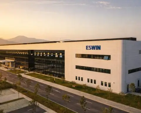
- A government-linked report confirmed that ESWIN’s silicon wafer facility in Wuhan has begun construction following approval of a key project filing.
- Investors face a tough call: a major capacity expansion looms while the company continues to predict losses.
The Hubei Province Department of Economy and Information Technology reported that Xi’an ESWIN Material Technology Co., Ltd. Class A has kicked off construction on its Wuhan silicon wafer base. This costly expansion might influence sentiment when A-shares resume trading on Monday. jxt.hubei.gov.cn
Timing is crucial. Large wafer projects often shift forecasts on production, client acquisitions, and funding—particularly for newer STAR Market entrants still ramping up. Investors want to know if this signals real momentum or merely increased spending.
On Jan. 21, the company forecasted 2025 revenue around 2.65 billion yuan, with a net loss to shareholders near 738 million yuan—about the same as last year. It pointed to sluggish pass-through of recovering end-demand, a second plant still ramping up, and hefty fixed costs plus R&D expenses as drivers of the losses. Still, it highlighted that operating cash net inflow remained positive. Qixin PDF
ESWIN shares ended Friday at 26.29 yuan, slipping 0.79% from the previous close of 26.50. During the session, the stock fluctuated between 25.71 and 26.98 yuan, according to data. Investing.com
Zhidian Caijing said the project cleared its first-phase filing, a key registration step in China’s investment approvals, and construction is underway with an estimated 2.5 billion yuan investment. The report also noted that the project entities have been registered in Optics Valley. Sohu
The Wuhan facility was initially mentioned in a Dec. 2 company announcement linked to a deal with Wuhan Optics Valley Semiconductor Industrial Investment Co., Ltd. ESWIN revealed the project aims to produce 12-inch silicon single-crystal polished wafers and epitaxial wafers — which include an extra grown layer used in specific chip manufacturing steps — targeting logic and memory chips as well as other devices. CLS
The company revealed plans to reach a capacity of at least 500,000 wafers per month, aiming to boost its total output to roughly 1.7 million wafers monthly once the expansion wraps up. Sina Finance
ESWIN’s ticker carries a “-U” suffix, a STAR Market marker for firms that went public ahead of profitability, per Shanghai Stock Exchange rules. SSE
In notes from a Dec. 25 investor meeting, ESWIN outlined a “15-year” strategy focused on establishing “2–3” manufacturing hubs for advanced 12-inch wafer fabs. Yang Chunlei and Wang Chen were named as company representatives present. Dfcfw PDF
The report also noted that ESWIN’s second factory aims to hit a monthly output of 500,000 wafers by the end of 2026, with consolidated profitability targeted for 2027. Dfcfw PDF
The downside is clear-cut: wafer demand could drop sharply, prices might remain stubbornly high, and major builds risk delays due to equipment delivery, customer qualification, or financing hurdles. Such a large project could also ramp up leverage if the cash burn continues.
Traders are eyeing Monday’s open in China to see if the construction start signals actual progress or spells new capex risk — and to catch any updates on financing details or the project timeline.
